


-
Call Us
T. : 0086-592-5657925
M. : 0086-1360-6089-112
-
Email Us
-
Skype
T. : 0086-592-5657925
M. : 0086-1360-6089-112
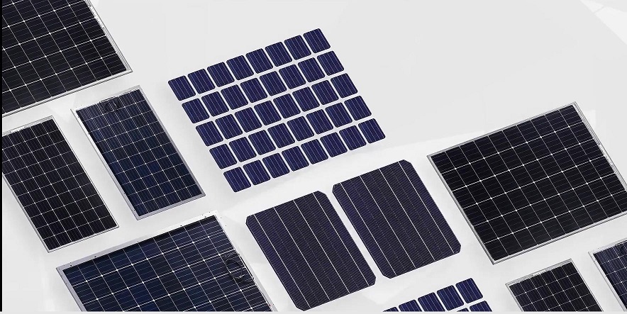
In July 2017, the company started the research and development of the N-type double-sided TOPCon solar panel cell. The front surface of the solar panel cell uses a boron diffused emitter and the back surface is a passivation contact structure of SiOx/n+ poly. The intrinsic poly-Si is deposited by LPCVD and then used Ion implantation is used for doping. Both the front surface and the back surface are H-type grid electrodes, which can generate electricity on both sides. This technical route is called J-TOPCon 1.0.
In 2019, the company took the lead in realizing the 1.5 GW mass production of N-type double-sided TOPCon cells, and the average conversion efficiency of mass production reached 22.5%. In June of the same year, the development of a new TOPCon technology based on plasma oxidation and plasma assisted in-situ doping (POPAID) began. The use of a chain platform to transmit the carrier board can simultaneously complete the tunneling of the oxide layer and the doped amorphous without breaking the vacuum. Silicon deposition, to achieve true no-winding plating, shortened the 12 manufacturing processes in TOPCon 1.0 to 9 processes, and the technical route was smoothly upgraded to J-TOPCon 2.0.
In 2020, J-TOPCon 2.0 technology will mature, which will promote the further improvement of N-type TOPCon solar panel cell efficiency, achieving the highest conversion efficiency of 24.5% and batch conversion efficiency.
In 2021, based on J-TOPCon 2.0 technology, began to build 182 large-size N-type double-sided TOPCon solar panel cell lines, and achieved a R&D efficiency of 25.4%. It was certified by the third-party China Institute of Metrology (NIM) and broke the record of TOPCon solar panel cell efficiency at that time.
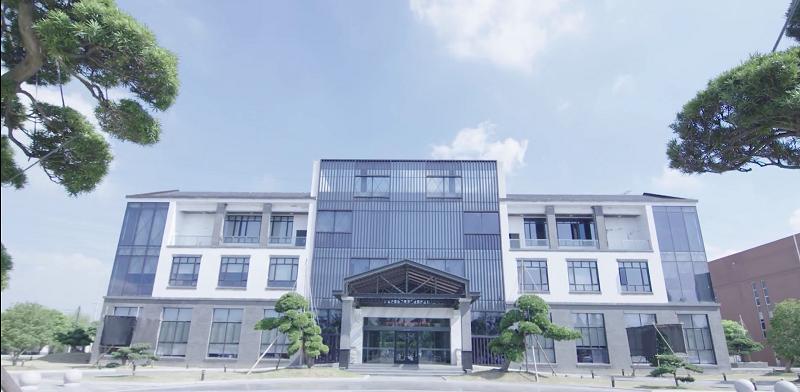
Room 2206, No. 6 Hubin East Road,Xiamen,China.
Mobile Phone : 0086-1360-6089-112
WhatsApp : +8613606089112
E-mail : 852966384@qq.com


Scan it